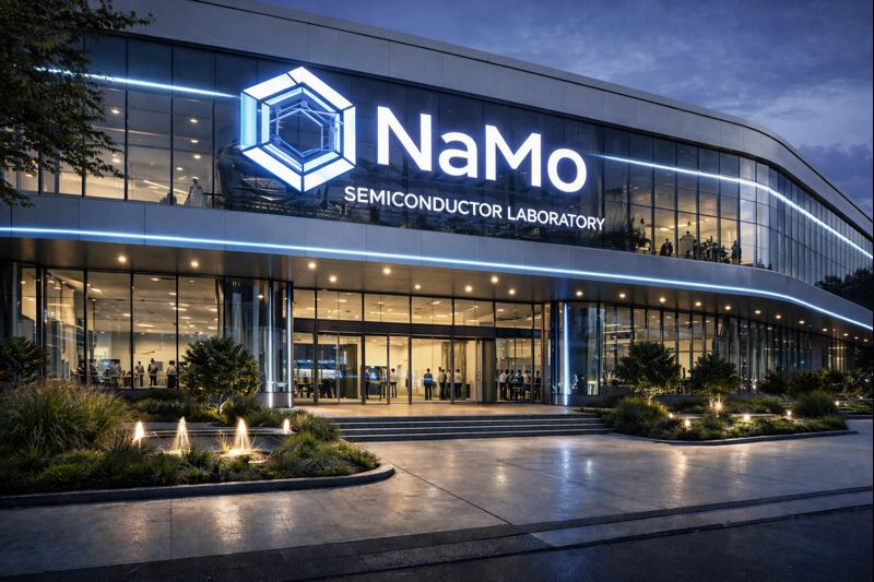
The recent approval of the NaMo Semiconductor Laboratory marks a transformative moment in India’s journey toward becoming a global leader in high-tech manufacturing. Strategically approved by the Union Minister of Electronics and IT, Ashwini Vaishnaw, in late 2025, this facility is designed to bridge the gap between theoretical academic research and practical industrial application. By establishing this state-of-the-art facility at IIT Bhubaneswar, the government is not just building a lab; it is laying the foundation for a self-reliant “Viksit Bharat” in the electronics sector. This initiative is a clear signal to the world that India is ready to move beyond chip design and master the complex art of fabrication and packaging.
As the global demand for semiconductors skyrockets, the NaMo Semiconductor Laboratory serves as a vital response to supply chain vulnerabilities and the rising need for indigenous technology. The facility will act as a premier hub for training the next generation of engineers, ensuring they are equipped with the skills required by modern fabrication units. This move aligns perfectly with the broader national vision of securing technological sovereignty and reducing dependence on foreign imports. By focusing on high-growth areas like Silicon Carbide (SiC) and advanced 3D packaging, the lab is positioning India at the cutting edge of the global semiconductor market.
-
The project is funded with an investment of ₹4.95 Crore under the MPLAD Scheme.
-
It aims to serve as a national hub for semiconductor skilling and R&D.
-
The lab will significantly boost the ‘Make in India’ and ‘Design in India’ missions.
-
It will play a critical role in developing talent for the OSAT and ATMP units across India.
India’s Leap into High-Tech: The NaMo Semiconductor Laboratory Approval
The approval of the NaMo Semiconductor Laboratory represents a bold step forward in India’s industrial evolution, transitioning the country from a consumer of technology to a creator of it. This laboratory is not an isolated project but a piece of a larger puzzle designed to make India a “Semiconductor Nation.” With the global chip market projected to exceed $1 trillion by 2030, India’s timely investment in such facilities ensures it captures a significant share of this growth. The lab will focus on high-end research that can be directly translated into commercial products, supporting both startups and established tech giants.
The Strategic Vision Behind the Initiative
The strategic vision for the NaMo Semiconductor Laboratory is to create a localized ecosystem where innovation can thrive without the constraints of global supply delays. By fostering an environment that encourages “First Time Right” design and fabrication, the government aims to lower the barrier of entry for Indian hardware startups. This vision emphasizes the importance of energy-efficient integrated circuits and high-power electronics, which are crucial for the future of electric mobility and renewable energy. The lab will essentially serve as an incubator for indigenous intellectual property in the semiconductor space.
A Major Milestone for the India Semiconductor Mission (ISM)
The establishment of the NaMo Semiconductor Laboratory is a crowning achievement for the India Semiconductor Mission (ISM), which has an outlay of ₹76,000 Crore. While large-scale fabs take years to build, this laboratory provides immediate hands-on experience to students and researchers, creating a ready-to-work force. It complements other ISM initiatives, such as the Design Linked Incentive (DLI) scheme, by providing the physical infrastructure needed for prototyping. This milestone proves that India is moving with “speed and power” to realize its ambitions in the semiconductor and electronics manufacturing sectors.
| Parameter | Details of NaMo Semiconductor Lab |
| Location | IIT Bhubaneswar, Odisha |
| Funding Source | MPLAD Scheme (Union Minister Ashwini Vaishnaw) |
| Total Investment | ₹4.95 Crore (Equipment: ₹4.6 Cr, Software: ₹35 Lakh) |
| Focus Areas | Chip Design, Fabrication, Testing, and Packaging |
IIT Bhubaneswar: The Ground Zero for Semiconductor Excellence
Choosing IIT Bhubaneswar as the host for the NaMo Semiconductor Laboratory was a strategic decision based on the institute’s proven track record in materials science and electronics. The campus has quickly become a center of excellence, attracting top-tier faculty and research grants that make it the ideal environment for high-precision engineering. As the “Ground Zero” for this initiative, the institute will provide the necessary academic rigor and research discipline to make the lab a success. It will serve as a lighthouse, guiding other technical institutions in the eastern region toward the semiconductor frontier.
Why IIT Bhubaneswar Was Chosen as the National Hub?
IIT Bhubaneswar was selected due to its robust infrastructure and the proactive support of the Odisha state government, which recently updated its semiconductor policy. The institute’s location in a growing industrial corridor allows for a direct “lab-to-market” pipeline, where researchers can collaborate with local manufacturing units. Furthermore, the institute’s commitment to interdisciplinary research ensures that the NaMo Semiconductor Laboratory benefits from expertise in physics, chemistry, and electrical engineering. This holistic environment is essential for solving the complex challenges associated with modern chip fabrication.
Integrating with Existing Silicon Carbide Research & Innovation Centre (SiCRIC)
A key strength of the NaMo Semiconductor Laboratory is its integration with the existing Silicon Carbide Research & Innovation Centre (SiCRIC). Silicon Carbide is a “wide-bandgap” semiconductor that is superior to traditional silicon for high-voltage applications like electric vehicles (EVs) and power grids. By leveraging SiCRIC’s cleanroom facilities and specialized equipment, the new laboratory can accelerate its work on next-generation power electronics. This synergy makes IIT Bhubaneswar a unique player in the global semiconductor landscape, capable of tackling niche but high-value markets.
-
IIT Bhubaneswar already hosts state-of-the-art cleanroom facilities.
-
SiCRIC focuses on Silicon Carbide (SiC) compound semiconductors.
-
The integration allows for cross-disciplinary research on power ICs.
-
It positions Odisha as the gateway to the East for semiconductor manufacturing.
Building the Talent Pipeline: Skilling India’s Youth for 2026 and Beyond
One of the most significant contributions of the NaMo Semiconductor Laboratory will be its role in closing the talent gap in the global tech industry. Currently, India accounts for 20% of the world’s chip design talent, but there is a desperate need for professionals who understand the fabrication and packaging aspects. The lab will provide intensive, hands-on training that goes far beyond textbook learning, allowing students to work with industry-grade tools. This talent pipeline will be the fuel that drives India’s semiconductor manufacturing units for the next decade and beyond.
Equipping Engineers with Industry-Ready Design and Fabrication Skills
The curriculum at the NaMo Semiconductor Laboratory is designed to mirror the requirements of modern semiconductor foundries and packaging houses. Engineers will be trained in advanced lithography, etching, and chemical vapor deposition techniques, which are the building blocks of chip making. By the time students complete their training at the NaMo Semiconductor Laboratory, they will be ready to contribute to the global workforce without needing extensive retraining. This “industry-ready” focus is what will make Indian engineers highly sought after in the international market.
Infrastructure and Investment: State-of-the-Art Tools for Indigenous Innovation
The success of any high-tech initiative depends on the quality of its infrastructure, and the NaMo Semiconductor Laboratory is equipped with the best tools available. With a dedicated budget for both hardware and software, the lab ensures that researchers are not limited by outdated technology. The investment of ₹4.95 Crore is specifically allocated to ensure that the lab meets international standards of precision and cleanliness. This investment is a down payment on India’s future as a tech superpower, providing the “heavy lifting” needed for indigenous chip development.
Allocations for Advanced Hardware and Electronic Design Automation (EDA) Software
A major portion of the funding for the NaMo Semiconductor Laboratory—approximately ₹4.6 Crore—is dedicated to purchasing advanced fabrication and testing equipment. This includes precision machines that can handle the delicate tasks of wafer processing and circuit etching. Additionally, ₹35 Lakh has been allocated for high-end EDA software, which is used to design and simulate chips before they are ever built. This combination of powerful hardware and cutting-edge software allows the NaMo Semiconductor Laboratory to handle the entire “cradle-to-grave” cycle of semiconductor development.
The Role of the MPLAD Scheme in Funding India’s Future Tech
Interestingly, the NaMo Semiconductor Laboratory is funded through the Members of Parliament Local Area Development (MPLAD) scheme, specifically from the funds of Ashwini Vaishnaw. This highlights a unique model of using local development funds for national-level high-tech infrastructure. It shows that even localized funding can have a massive impact when directed toward strategic sectors like electronics. This funding model might serve as a template for other regions to build specialized research labs that contribute to the national India Semiconductor Mission.
| Category | Budget Allocation | Purpose |
| Equipment | ₹4.6 Crore | Precision machines for fabrication and testing |
| Software | ₹35 Lakh | Advanced EDA tools for chip design/simulation |
| Facility | Integrated with SiCRIC | Utilizing existing cleanroom and R&D space |
| Total | ₹4.95 Crore | Comprehensive semiconductor development hub |
Strategic Impact on ‘Make in India’ and ‘Design in India’
The NaMo Semiconductor Laboratory is a powerful catalyst for the government’s flagship ‘Make in India’ and ‘Design in India’ programs. By providing a local facility for testing and prototyping, it reduces the time and cost associated with sending designs abroad for fabrication. This encourages more domestic companies to enter the semiconductor space, knowing they have world-class support right in Odisha. The lab’s output will directly feed into the manufacturing ecosystem, creating a virtuous cycle of domestic innovation and production.
Reducing Global Supply Chain Dependence Through Local Manufacturing
The global chip shortage of recent years proved that over-dependence on a few countries for semiconductors is a major risk to national security. The NaMo Semiconductor Laboratory is a key part of India’s strategy to build a localized supply chain that can withstand global shocks. By mastering the fabrication of essential components, India can ensure that its automotive, defense, and telecommunications sectors are never held hostage by global shortages. This move toward self-reliance is not just about economics; it is about protecting the nation’s technological sovereignty in an uncertain world.
Catalyzing Odisha’s Emerging Role as a Semiconductor Powerhouse
With the establishment of the NaMo Semiconductor Laboratory, Odisha is rapidly emerging as a new “Silicon Valley” of the East. The state has already secured approval for major projects like SiCSem and 3D Glass Solutions, which will create thousands of jobs. The lab at IIT Bhubaneswar will act as the “brain” of this ecosystem, providing the R&D and skilled workers needed to sustain these massive investments. This transformation is turning Odisha into a preferred destination for global semiconductor giants, significantly boosting the state’s economy and prestige.
-
Odisha has secured ₹4,600 Crore in new semiconductor investments.
-
The state’s new semiconductor policy offers relocation and R&D support.
-
Make in India initiatives will benefit from local chip supply.
-
Indigenous chips will power Indian-made EVs and missiles.
The Future Outlook: Transforming India into a Global Chip Design Hub
The long-term goal of the NaMo Semiconductor Laboratory is to help transform India into a global hub for end-to-end chip design and manufacturing. While India has been a design powerhouse for decades, the addition of fabrication and packaging capabilities completes the value chain. By 2030, the Indian semiconductor market is expected to reach $110 billion, and facilities like this lab will be the primary drivers of that growth. The future looks bright as the lab begins to produce the IP and talent that will define the next generation of global technology.
Empowering 100+ Universities with Next-Gen Semiconductor Technology
One of the most ambitious aspects of the NaMo Semiconductor Laboratory project is its plan to empower students from over 100 universities. The lab will share its resources and knowledge through collaborative research programs and faculty exchange initiatives. This “hub-and-spoke” model ensures that the benefits of the NaMo Semiconductor Laboratory reach every corner of the country, not just the IITs. By democratizing access to semiconductor technology, the government is ensuring that every talented student in India has a chance to contribute to the nation’s high-tech future.
Long-Term Benefits for the AI, IoT, and Automotive Electronics Sectors
The chips developed at the NaMo Semiconductor Laboratory will have far-reaching impacts on various high-growth sectors. In Artificial Intelligence, the lab’s work on energy-efficient circuits will help power the next generation of AI edge devices. For the Internet of Things (IoT), the lab will focus on low-power sensors that can be used in smart cities and precision agriculture. In the automotive sector, the research on Silicon Carbide will be vital for the high-power electronics required by electric vehicles, making the NaMo Semiconductor Laboratory a central player in the global green transition.
Doon Defence Dreamers: Training Officers for a Tech-Ready India
Doon Defence Dreamers has established itself as the premier destination for defense aspirants, earning the reputation of the best NDA coaching in Dehradun. With India making giant strides through initiatives like the NaMo Semiconductor Laboratory which is a research and development facility focused on semiconductor chip design and fabrication.
The academy has consistently delivered record-breaking results, transforming the dreams of thousands of young students into a reality of service to the nation. The institution’s success is built on a foundation of rigorous academic discipline, specialized SSB training, and a focus on the evolving technological needs of the Indian Armed Forces.
The academy’s achievements reflect its commitment to excellence, combining traditional teaching methods with modern pedagogical tools. By maintaining a high standard of training and mentorship, it has become a powerhouse for producing commissioned officers who are ready to lead in a high-tech era.
-
Record-Breaking Written Results: The academy recently celebrated an unprecedented 710+ written selections in the NDA/NA (II) 2025 examinations, the highest in the region.
-
Massive Officer Production: Within just the last two years, over 752 aspirants guided by the academy have successfully transitioned into officer-level roles in the Army, Navy, and Air Force.
-
Unmatched SSB Recommendations: In a single month, the institution achieved a staggering 35 SSB recommendations for the NDA 155 batch, proving the efficacy of its personality development modules.
-
International Recognition: Doon Defence Dreamers was honored with the prestigious Jagran Achiever Award 2025 on an international stage, recognizing its excellence in defense education.